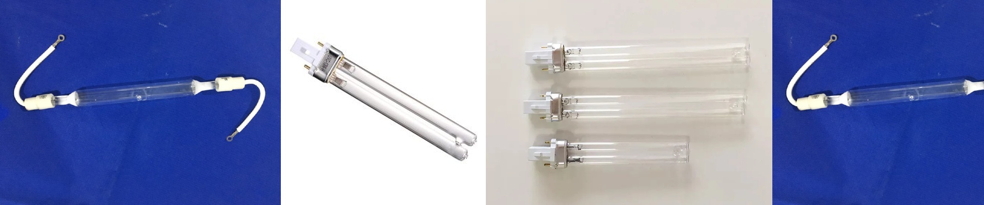
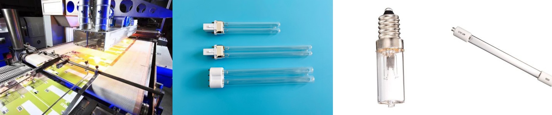
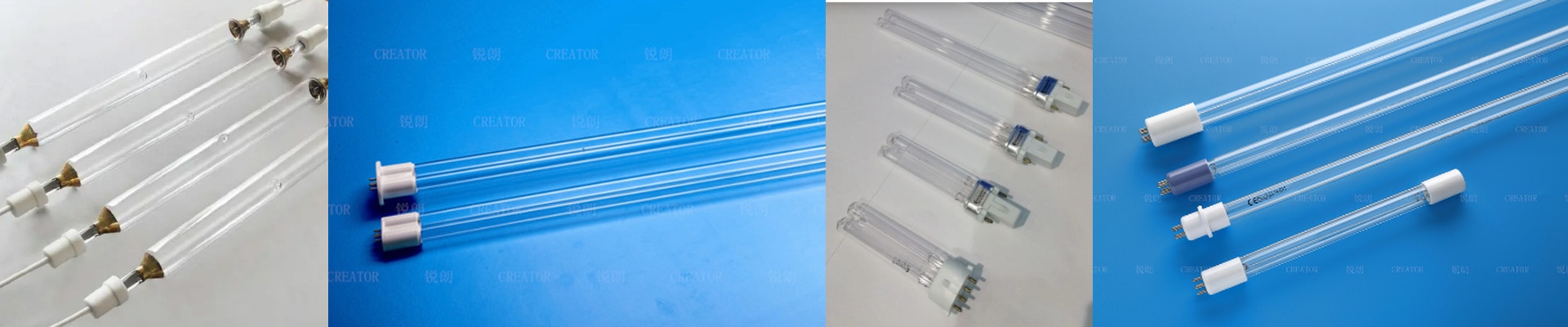
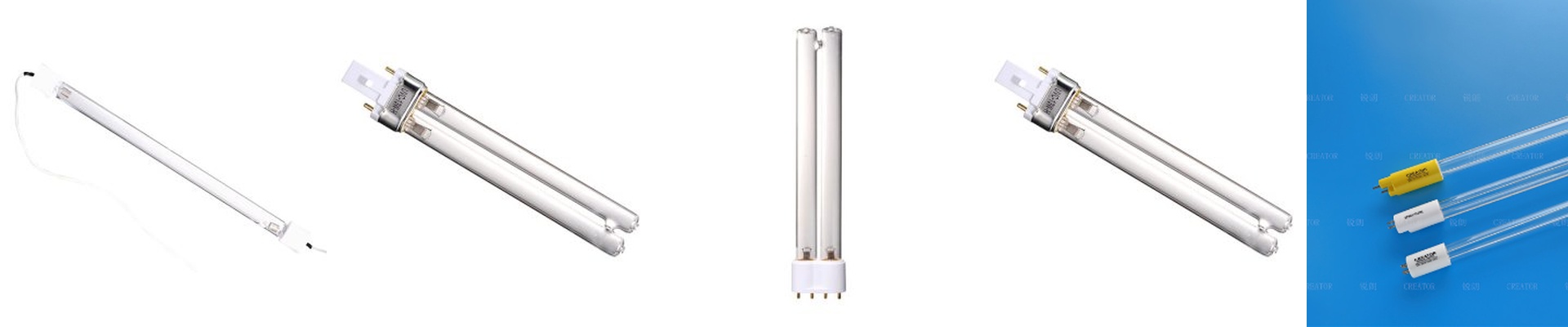
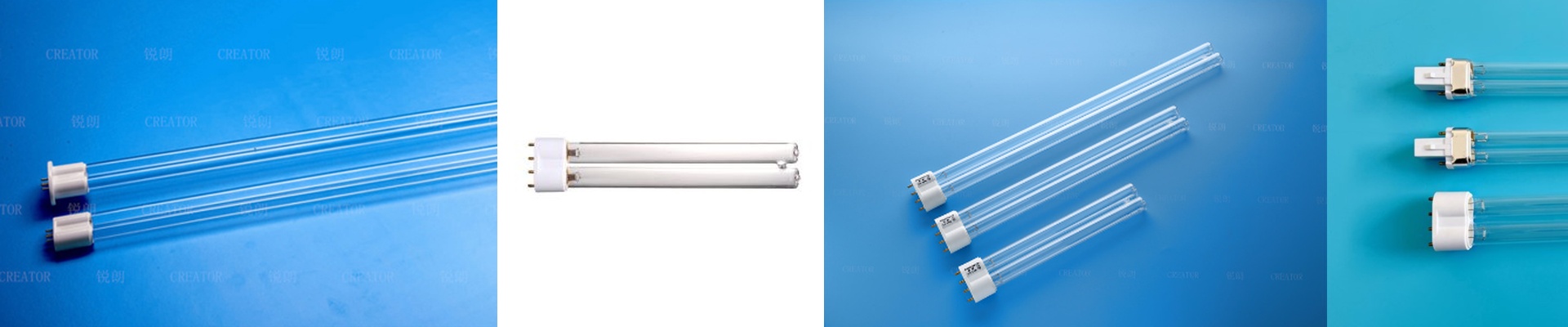
On the PCB line, the UV curing stage isn’t a “nice-to-have.” It’s the pinch point. When the lamp is CE-marked and putting out stable, repeatable power, the line keeps moving. When you’re running uncertified lamps that sag and drift, you pay for it in scrapped boards, rework, and customs holds that stop global shipments cold. What actually matters under the hood We build these UV lamps for PCB work around high-pressure mercury vapor arc tubes and dichroic reflectors, tuned so the spectral output leans hard on 365nm. That’s what gets the photoinitiator going deep. Peak irradiance is specified right at the arc plane—not hand-waved. You get consistent energy density in mJ/cm² across the board, so cross-linking happens fast without cooking the material. Power density is matched to line speed, and the housing is set up for repeatable focus and heat control. Why this matters in real production CE certification isn’t paperwork for the sake of paperwork. It’s your ticket to EU compliance and safer cross-border movement. With a CE-marked system, you cut compliance risk, dodge shipment delays, and keep your audit trail clean. And the lamp’s spectral stability shows up directly as process Cpk. Solder mask, legend ink, and adhesive layers cure consistently, even when you’re pushing throughput. The payoff is fewer rejects, predictable lamp-to-lamp uniformity, and less energy burned per cured panel. A few shop-floor details that bite if you ignore them Installation tolerances are not optional. Keep the arc-to-substrate distance within the spec window, or irradiance drops off and the cure goes uneven. Before the first run, verify the machine interface dimensions and make sure the reflector alignment is spot-on. The lamp is ozone-free, but you still need proper exhaust. It handles the heat and keeps any volatiles from the ink or resin from hanging around where they don’t belong.